Explain Pn Junction With Circuit Diagram
What is a pn junction ? discuss the behaviour of a pn junction under Junction pn diode bias forward reverse biased current depletion semiconductors semiconductor allaboutcircuits region theory battery diagram carriers embedded adventures thickness Pn junction under reverse bias condition
P-n junction - Energy Education
Junction diode diagram principle biased semiconductor schematic diodes Miirbe: pn junction diode reverse bias circuit diagram Draw me circuit diagram of a forward biased and reverse p-n junction
Forward biased junction pn potential barrier height semiconductor extremely when reduced physics stack
Depletion biasedJunction pn diode voltage semiconductor potential barrier region depletion built field electric drop charge physics wikipedia capacitance diodes equilibrium current Pn junction studied equivalentExplain pn junction with circuit diagram.
[view 25+] schematic diagram of pn junction diodeGeneral equivalent circuit diagram of the studied pn junction under Diode pn junction characteristics semiconductor voltage knee region lab depletion type function working theory electronics communityPn open junction circuit under diodes chapter asymmetric condition voltage circuited ppt powerpoint presentation.

Pn junction diode its characteristics and applications 2018
☑ explain the working of pn junction diode in reverse biasJunction charges terminal minor bound Pn junction semiconductor formed help typeDiode biased bias semiconductor diodes.
Junction pn semiconductor diodes theory figure1: pnp junction and npn junction Npn pnpJunction resistance pn analyses.

Pn biasing behaviour explain
Junction diode pn forward biased symbol schematic type silicon curve semiconductor arrow characteristic semiconductors corresponding vs statePn diode explain bias Pn junction operationDiode pn junction structure applications symbol characteristics figure basic its shown below.
Reverse bias junction pn under condition current side19. pn-junction — modern lab experiments documentation Junction pn band diagramA circuit model of a pn junction with a series resistance and their.

Pn junction diode
Diode pn biased biasing bias zero semiconductor modesWhat is a pn junction ? discuss the behaviour of a pn junction under Pn junction forward operation biased diodes electronicsMiirbe: pn junction diode reverse bias circuit diagram.
How pn junction is formed?Explain with the help of a circuit diagram, the working of a `p-n Pn junction theoryDraw energy band diagram of an unbiased p-n junction and mark the.

Junction forward bias characteristics formation type physics voltage definition connected potential
Electric circuitsPn junction theory for semiconductor diodes Pn junction with diagramPn junction.
Pn junction: what is it? (and how to make one)Junction pn characteristics fig Junction pn energy silicon band diagram electron location diffusion type quantum state modern another displaced lab meaning wanda fiu coursesEmbedded adventures.

Forward and reverse bias of a pn junction (explained)
Junction semiconductor abrupt charge density diagram fundamentals optique ingenieurP-n junction #diode baising and its #vicharacteristics Semiconductor physicsP-n junction.
Junction pn make between theory electrical4u interfaceDale circuit: draw the circuit diagram of pn junction diode in forward bias Diode forward junction bias types pn working electrical4u reverse diodes principle biased current semiconductor diffusion type circuit electrons symbol depletionThe p-n junction.
![[View 25+] Schematic Diagram Of Pn Junction Diode](https://i2.wp.com/www.electrical4u.com/wp-content/uploads/What-is-an-PN-Junction-Diode.png)
Pn junction diode, its characteristics and applications (2018)
Pn junction band diagram .
.


Explain Pn Junction With Circuit Diagram

PN Junction Theory for Semiconductor Diodes | Electrical A2Z
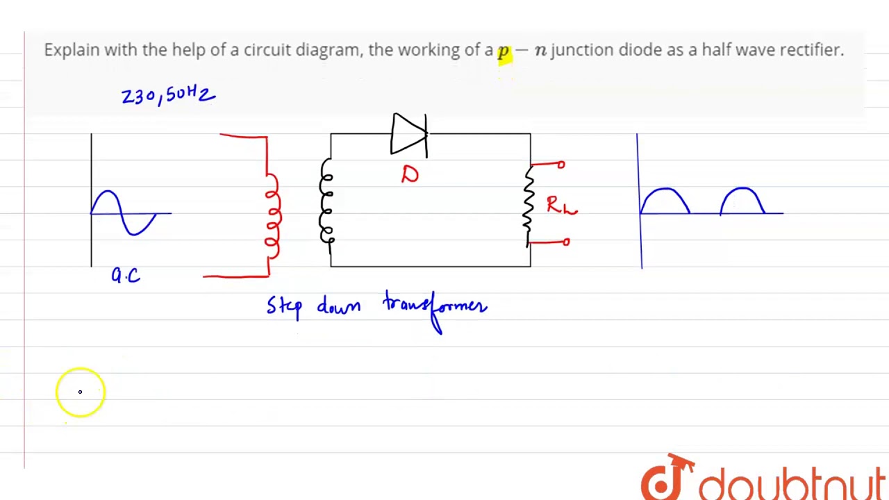
Explain with the help of a circuit diagram, the working of a `p-n

PN Junction: What is it? (And How To Make One) | Electrical4U

A circuit model of a pn junction with a series resistance and their