Forward And Reverse Bias Circuit Diagram
Circuit with voltmeter and ammeter Circuit reverse bias diagram diode lab forward characteristics tech Reverse diode junction semiconductor avalanche capacitance pn biased depletion biasing region diodes physics breakdown voltage zener electrons transition type bias
How to find the Diode voltage in forward-reverse bias combination
Pn junction diode: forward and reverse bias characteristics Solved 2 1. p-n junction diode characteristics aim:-to Transistor basics
Transistor biasing
Dioda reverse bias dan forward bias risetHow to find the diode voltage in forward-reverse bias combination Diode reverse biasing download scientific diagramReverse bias pn under diode junction biased region gif.
Circuit diagram: a) forward bias: (0-200 ma 1 κω wSchematic diagram of forward biased diode Bias reverseReverse forward biasing circuit diode junction distinguish diagrams between bias sarthaks help.

Pn junction under reverse bias condition
Pn junction diode(i) with the help of circuit diagrams distinguish between forward Difference between forward and reverse biasing with comparison chartSolved consider the following schematic. the forward-bias.
Tech lab: experiment 3: v-i characteristics of semiconductor diode (geWhat is a pn junction diode, how it is formed, also i-v characteristics Bias reverse forward junction diode silicon biased pn semiconductor diodes diagram reversed physics region chapter type creations current emitting themDale circuit: draw the circuit diagram of pn junction diode in forward bias.

Reverse junction bias electric field
Diode forward bias & reverse bias circuitReverse and forward bias ~ pooza creations Reverse bias junction pn under condition current sideWhat is forward and reverse current?.
Semiconductor physicsSchematic diagram of forward biased diode A bias circuit and b start-up circuit [19]Circuit diagram zener diode.

Bias reversed pn
Electronics: pn jnction diode under reverse biasForward bias, reverse bias and their effects on diodes Schematic diagram of forward biased diodeForward biasing reverse difference between circuit bias diode vs region comparison voltage type barrier potential circuitglobe.
Get 42 zener diode reverse bias circuit diagramP-n junction with reversed bias. energy band diagram is also shown Miirbe pn junction diode forward bias diagramReverse biasing forward circuit between bias difference current definition differences key potential barrier.

Difference between forward & reverse biasing with comparison chart
Transistor biasing bias bjt biased instrumentationtools engineeringtutorialDifference between forward & reverse biasing with comparison chart Diode pn semiconductor junction layer depletion working reverse bias characteristics flow physics battery lab electronics biasing circuit circuitspedia type chooseElectronic – why is the voltage across the depletion layer higher than.
What is reverse bias p n junction?Bias reverse forward junction gif basics transistor fig .


Schematic Diagram Of Forward Biased Diode - Wiring Diagram Line

PN Junction diode: Forward and Reverse bias characteristics

Difference Between Forward & Reverse Biasing with Comparison Chart

Dioda Reverse Bias Dan Forward Bias Riset - Riset

Solved Consider the following schematic. The forward-bias | Chegg.com

What is Reverse Bias p n Junction? - Circuit Globe
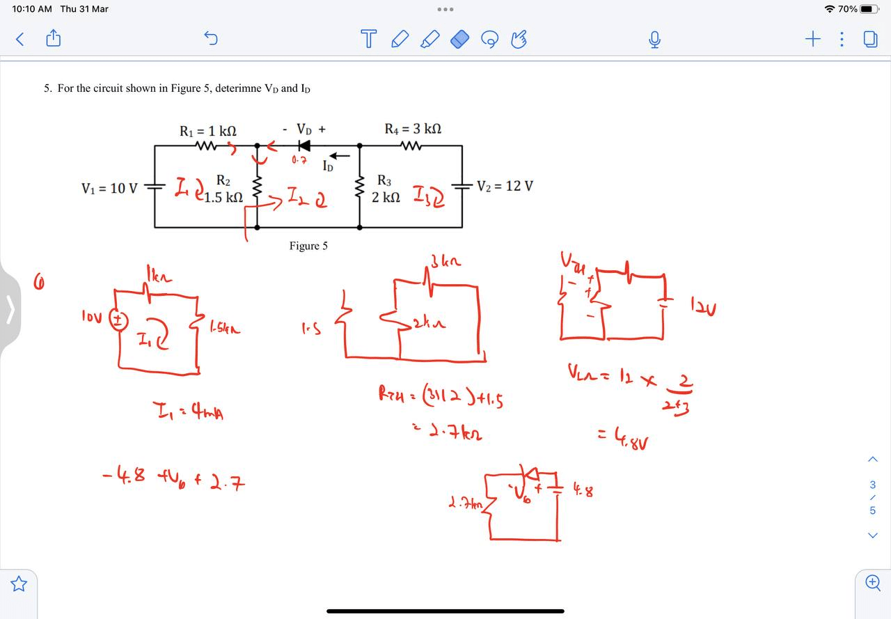
How to find the Diode voltage in forward-reverse bias combination